車祐成 (Karras Che)
E-mail: [email protected]
Now: Process Integration Engineer (110→40 nm Driver IC)
Process Engineer ( N5 → N3 Wet Clean )
X-ray analysis (XRD , XAS , & XPS)
Work Experience
Powerchip Semiconductor Manufacturing Corporation
Process Integration Engineer, Nov 2021 ~ Now
300mm Technology Foundry (Transfer and Production Integration )
■ Device WAT Window tunning and troubleshooting.
■ Process Design of Experiment (DOE)
■ Inline and Yield CIP improve.
Achievement:
(1) The new Device Vt/Ids/Ioff shift is improved by designing the process Implant/Thin Film DOE.
(2) Yield improved~1% through the design of BEOL WET/Thin Film Continuous Improvement Processes (CIP) for defect model improvements in the cleanliness of process equipment.
(3) The design improvement of the BEOL Cu process CIP enhances the low yield~10%.
Taiwan Semiconductor Manufacturing Corporation
Process Engineer, Mar 2020 ~ Jul 2021
MEOL HK Metal Gate Wet Clean Process Engineer from N5 to N3 technology
■Wet clean/etch tool maintenance and Productivity management.
■Inline/Offline SPC management and troubleshooting.
■Co-work with equipment engineer, process integration engineer to solve issues.
Achievement:
(1) N5 metal gate defect solution by studying the defect physical / chemical properties and designing continuous improvement process (CIP) .
(2) Design of Experiment (DOE) for offline wafer Q-time effect issue.
(3) New tech N3 tool wet etching rate improvement.
National Synchrotron Radiation Research Center (NSRRC), Research Assistant Student, Aug 2015 ~ Oct 2019
Research:
Electrochemical energy storage material research combined with synchrotron radiation_ X-Ray Diffraction ,X-Ray Absorption Spectroscopy and X-Ray Photospectroscopy analysis.
Publication:
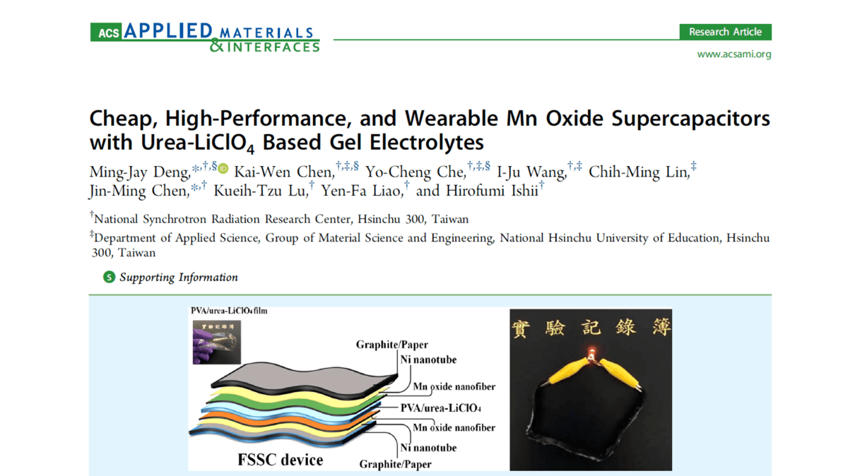
M.-J. Deng*, K.-W . Chen, Y.-C. Che,I.-J. W ang, C.-M. Lin,J.-M. Chen, K.-T. Lu, Y .-F. Liao, and H. Ishii, ACS Appl. Mater. Interfaces 2017, 9, 479−486
The experience of oversea research:
To analyz the material of supercapacitor by using 8 GeV energy synchrotron radiation at Spring-8 in Japan .
Achievement
M.-J. Deng*, K.-W . Chen, Y.-C. Che,I.-J. W ang, C.-M. Lin,J.-M. Chen, K.-T. Lu, Y .-F.Liao, and H. Ishii, ACS Appl. Mater. Interfaces 2017, 9, 479−486
2018年中華民國介面科學學會年會既科技部計畫成果發表會--口頭發表_優勝
Education
National Tsing Hua University
(MS) Department of Engineering and System Science
2017.09 ~ 2019.08
National Tsing Hua University
(BS)Department of Applied Science
2013.09 ~ 2017.08

Skills
Professional Field
1.Energy Materials
2.Electrochemical Analysis
3.X-ray (XRD,XAS & XPS)
Semiconductor Process
1.Physics of Semiconductor Devices
2.Integration Process
3.N5-->N3 Wet Clean MEOL Process
Language
1.Chinese
2.English
Autobiography
[Career Experience]
My first career experience was in the WET Clean Process Engineer. In addition to handling complex affair, I also had to delve into literature in that field and collaborate with different departments to generate new ideas to solve problems, design improvement experiments DOE/ CIP , It was a specialized role that required expertise. Currently, I am working in Process Integration Engineer, which involves a broader range of responsibilities. I am responsible for handling (1) Platform Transfer and (2) Mass Production stages.
(1) PlatformTransfer primarily involves working on new technology platforms for Tape Out. In the initial stage, I have to confirm the Process Design Kit (DRC, EDR, SPICE Model...), conduct pi-run processes, and analyze electrical windows. During this period, I solve Vt offset issues and Ioff leakage by studying the characteristics of the device and corresponding impacting processes such as Implant, Thin Film .
(2) In the Mass Production Stage, my task is on inline Cpk/defect analysis and sorting common tools to improve yield. With my previous process experience and expertise in Wet Clean, I can design BEOL WET/Thin Film CIP to improve process cleanliness targeting defect models.
[Efficiency Management]
<Learn → Communicate → Select & Observe → Work Efficiency>
In the workplace, tasks are not only complex but also urgency. Being chased by work is part of daily life. Therefore, how to allocate time and communicate with others has become a learning topic for me. In my career life, through observing and learning from my colleagues, I have come to understand the importance of thinking ahead before starting a task, choosing the best time to prioritize important matters, observing for shortcuts, or establishing my own set of SOP. This enables me to quickly get on track, improve my personal work efficiency, and increase productivity .
