林庭揚 (Ting Yang, Lin)
Over 7 years of semiconductor integration experience, and successful Tape-Out new products to 5nm from 90nm and mass production (including logic and more than moore products). Successfully improve product yield through data analysis and DOE, and enhance process tolerance. "Teamwork" is very important to me both in the graduate school and in the company. I hope that I have opportunity to try my best for your company with my extensive experience.
Process Integration Engineer, TSMC,
Tainan, Taiwan
[email protected]
+886 963958505
Skills
Semiconductor (5nm~90nm)
- Device engineering
- Semiconductor Process
- WAT Analysis
- Yield Analysis
- Process Quality Test
Manufacturing
- Statistical Process Control (SPC)
- Cp/Cpk
- Failure Mode and Effects Analysis (FMEA)
- Design of Experiments (DOE)
- PDCA
- 3-Leg-5-Why
- 8D
- Pareto Chart
- Box Plot & Normal Quantile Plot
Failure Analysis Tool
- JMP software
- Transmission Electron Microscopy (TEM)
- Energy-dispersive X-ray spectroscopy (EDX)
Work Experience
TSMC, Process Integration Engineer Nov 2014 ~ Present
- 5nm process experience for new product tape-out, yield/device improvement, process optimization and risk assessment.
- More than moore products' experience including 40/55/80nm high voltage (panel driver),
90nm eDRAM and 65nm automotive products.
- Yield/ device troubleshooting in semiconductor process and coordinating cross team (Module/ Device/ Defect/ Product) to propose possible solution.
- Design, execute and analyze experiment to find out process sweet spot for process window assurance.
- Good for customer management: technical support, successful new tape-out pilot run, device window optimization and continue improvement plan.
- Mass data analysis: inline/WAT/CP/FT data integrated analysis by EDA tool -- Implement FA skill for chip failure mechanism analysis, such as FIB/SEM/TEM/EDX,etc.
Award & Honor (TSMC)
- 2019 1H Engineering Contribution Award (Quality Improvement), 2nd Award, 2019
- Success tape-out customer 1st 40nm HV product, yield is over 90%, and pass customer product quality test.
- (5nm) Found wafer edge low yield caused by rework effect
- (5nm) Found chronic wafer center low yield caused by device profile and tool issue
- (40nm) Found and reduce the device leakage.
- (55nm) Improve wafer edge yield loss due to leakage and process weakness by wafer uniformity increment.
Education
National Cheng Kung University (NCKU)
Master's Degree, Electrical and Electronics Engineering, 2012 ~ 2014
Design and Verification of the Control Procedure of Attitude Determination and Control Subsystem for Nanosatellite.
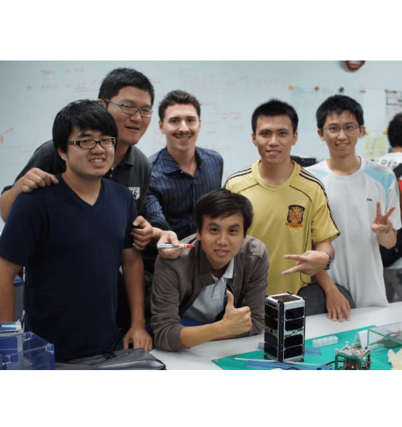
- Participate 1st cubesat (PACE) make and launch
- Japan Satellite Design Contest: lead graduate and college students to do engineering design
- Phoenix (QB50 project): Be responsible for attitude determination and control system
- Matlab teaching assistant
National Cheng Kung University (NCKU)
Bachelor's's Degree, Systems and Naval Mechatronic Engineering, 2008 ~ 2012
Award & Honor (NCKU)
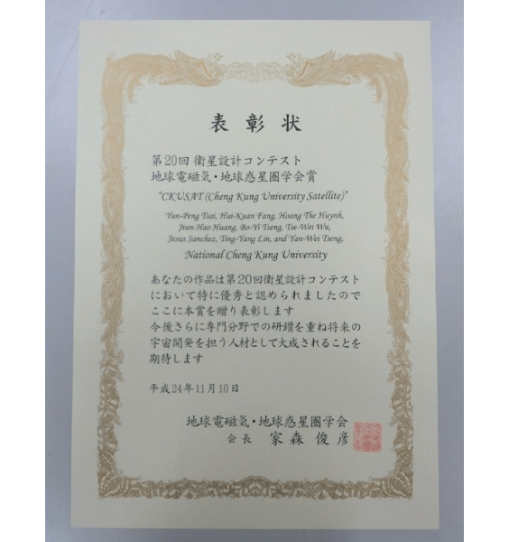
- The 20th Japan Satellite Design Contest, 1st Award, 2012
- Participate to manufacture 1st nanosatellite by students.