
- Jobs
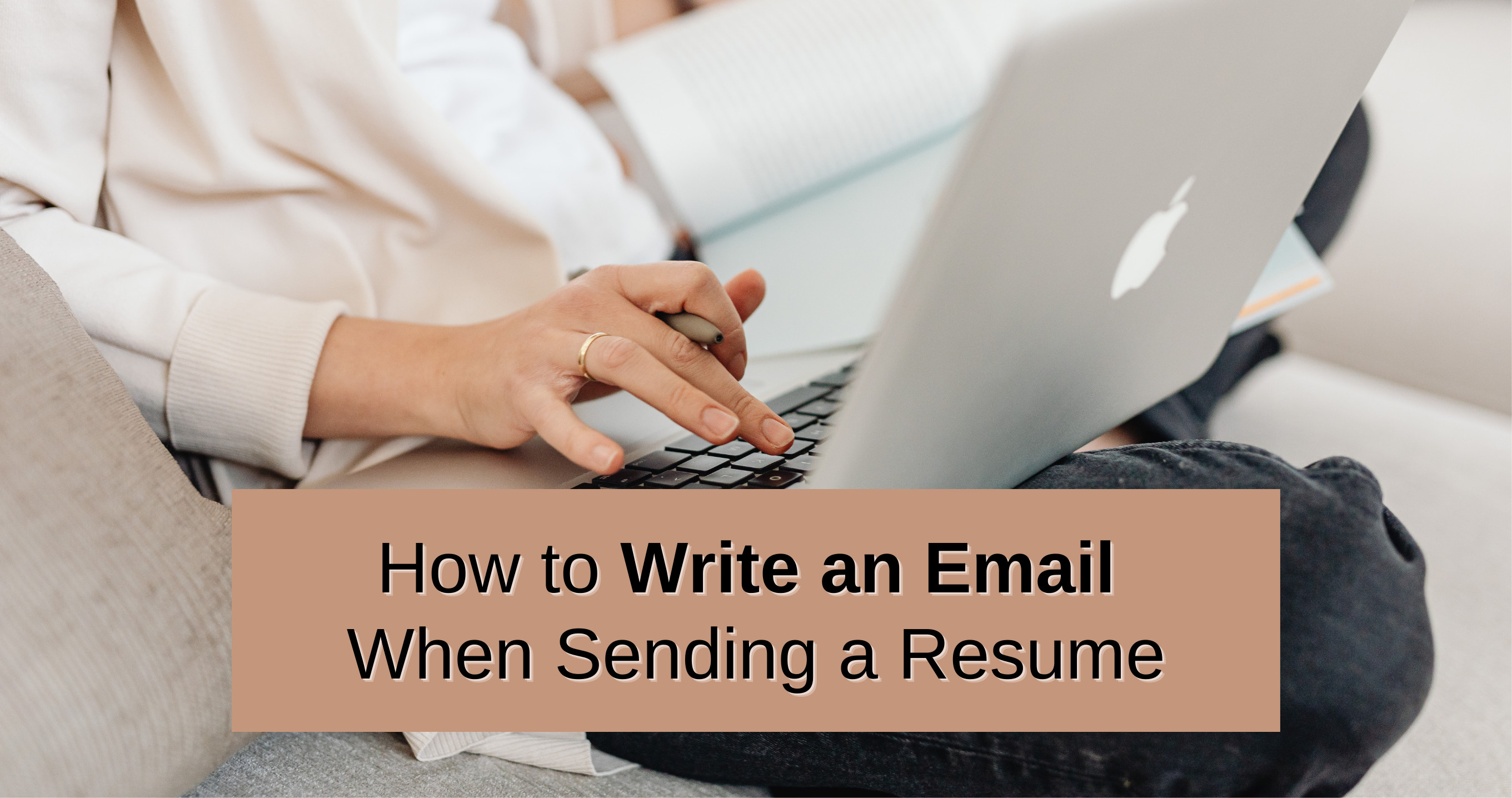
 ResumeCreate your job-winning resume using our free resume builder.
 PortfolioShowcase your skills and projects with a professional portfolio.ResumeCreate your job-winning resume using our free resume builder.Resume BuilderMake a resume for free.Resume TemplatesAccess our extensive library of professional & ready-to-use templates.Resume ExamplesGet inspired by real resume examples to create your own.Occupation GuideAccess resume writing guides tailored for different professions.Resume HelpGet expert advice on all things resume from our team of recruitment specialists.
- ResourcesSuccess StoriesBusiness ExcellenceAbout CakeResumeFeatured Reads
- Hire
- Download our App


Yu-Ta,Wu
Metrology Engineer
Experienced metrology engineer with 6+ year of process technologies in Taiwan Semiconductor Manufacturing Company (N06/N07/N22/N28).
3+ years in 6nm/7nm process, found path for optical metrology.
3+ years in 22nm/28nm litho-related metrology & 2nd mask quality sponsor.
Personality, good communicated with cross-department/learning fast/work smart/willing to accept new challenge.
Extremely interested in companies located in Taichung/Taipei/Taoyuan or the USA.
Taiwan Semiconductor Manufacturing Company(TSMC)
National Chiao Tung University
Taichung, 台灣
Professional Background
- Current status
- ProfessionSemiconductor Engineering
- FieldsSemiconductor
- Work experience6-10 years (6-10 years relevant)
- ManagementNone
- Skills
- LanguagesEnglish・IntermediateChinese・Native or Bilingual
- Highest level of educationMaster
Job search preferences
- Desired job typeFull-time・Interested in working remotely
- Desired positionsMetrology Engineer
- Desired work locations
- FreelanceNon-freelancer
Work Experience
Metrology Engineer (OCD)
•N6/N7 Optical Critical Dimension (OCD) metrology owner (Recipe/Quality Control/Productivity.etc)
•OCD 2D/3D library model building for inline new monitor create & path-finding.
•Co-work with PID/Module for OCD inline issue & metrology solution.
•Developed metrology methodology (ex:Machine learning for spectrum analysis , Sense-array .etc)
•N7 wafer container quality owner (Foup dimension/Inspection/AMC Gas analyzer)
Mask & Metrology Engineering
•N28 Critical Dimension Electron Microscope (CD-SEM) metrology sponsor.
•LIT defect scanner (Viper/OM) sponsor for lithography-related defect monitor.
•Thermal-wave (OP) sponsor for lithography photo-resist thickness defense.
•2nd version Mask qualified by handling experiment lot pi-run CD/KLA scan & WAT analysis .
Education
Master’s Degree
・
Display InstituteActivities and societies
Class president of Display Institute (2012-2014)
Bachelor’s Degree
・
Department of PhotonicsActivities and societies
Photonics Student Association member (2008-2009)
Dancing club member (2008)