
- Jobs
 ResumeCreate your job-winning resume using our free resume builder.
 PortfolioShowcase your skills and projects with a professional portfolio.ResumeCreate your job-winning resume using our free resume builder.Resume BuilderMake a resume for free.Resume TemplatesAccess our extensive library of professional & ready-to-use templates.Resume ExamplesGet inspired by real resume examples to create your own.Occupation GuideAccess resume writing guides tailored for different professions.Resume HelpGet expert advice on all things resume from our team of recruitment specialists.
- ResourcesSuccess StoriesBusiness ExcellenceAbout CakeResumeFeatured Reads
- Hire
- Download our App


CakeResume Talent Search
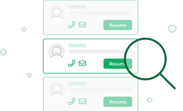
The Most Lightweight and Effective Recruiting Plan
Search resumes and take the initiative to contact job applicants for higher recruiting efficiency. The Choice of Hundreds of Companies.
- Browse all search results
- Unlimited access to start new conversations
- Resumes accessible for only paid companies
- View users’ email address & phone numbers
Definition of Reputation Credits
陳宇星 (Yu-Hsing Chen)
您好,我是陳宇星,,2015年來,在聯華電子/台灣積體電路擔任蝕刻製程工程師,
半導體開發經驗五年;職涯下一步有意往研發/整合職缺尋找,或歷練不同文化的公司的製程開發,如貴公司有這個機會,希望有彼此能配合的時間認識與了解,感謝!
半導體工程師(資歷五年) 1990/12/19 男性 代
Date of Arrival: 一個月內
Tainan,TW
Education
成功大學NCKU, 材料與工程學系MSE, 2009 ~ 2013
dance club 3rd Public Perform
成功大學NCKU, 材料與工程所MSE, 2013 ~ 2015
(micro plasma/OES/SEM/XRD/EDX/AFM/UV-visible)
The efficacy assessment of non-thermal micro-plasma in comparison with negative pressure treatment on healing diabetic wounds in mice
Experience
聯華電子UMC, 製程工程師process engineer, Nov 2015 ~ May 2018
1. inline CD /depth SPC maintain
2. weak pattern setup
3. cost reduction 80w/month
4. slot effect improve 50%
5. defect improvement from 5 to 3 count/ wafer
台灣積體電路公司, 製程工程師process engineer, Jun 2018 ~ Sep 2020
1. F18 N5 FEOL new tech transition
2. FINFET CD / depth SPC maintain
3. WPH improvement 50%
4.new tool import for production line expansion
5. DOE design uniformity improve 30%
6. Auto system coordinator and APC setup
Equipment
Process:
TEL SCCM/VIGUS/F1000 Hitachi 9012
Measurement:
(CDSEM/ SCD/ OP/ micro plasma/OES//EDX/AFM)
Skills
JIRA JMP
Data Analysis
Design of Experiment
SAS-EG
Excel VBA
Working efficiency
Language
English - Fluent
Taiwanese - Fluent
Mandarin - Fluent
自傳
出生於1990年,台南人,射手座B型。
個性活潑外向,平時喜歡打羽球和騎腳踏車。
目前在找第三份研發/製程相關工作。
2015/11~2018/05 聯華電子蝕刻二部製程工程師
近三年的工作經歷在半導體業
期間除了維持製程上的穩定外
主要業務在於
1.DOE手法改善40奈米線寬片與片的差異
2.缺陷新方式改善降低良率不良因子
3.控片成本降低(每個月80萬新台幣)
4.特殊量測圖形建立
2018/06~2020/09 台積電F18蝕刻一部製程工程師
轉到台積電後主要負責最新N5量產技術
主要業務在於
1. 5奈米從RD 端導入到量產階段
2.新機台評估與驗證
3.產出率提升50%
4.DOE手法改善5奈米線寬蝕刻均勻度
5. APC 建立與驗證
主要興趣在單車以及羽球、慢跑的領域,會希望在跟朋友狂歡後,保有與跟自己對話的角落,運動亦能維持健康與體態,才能在工作時更加專注。
在聯電與台積電近5年的工作經歷,是很好的人生歷練,然而 基於對其他領域與不同職缺求知若渴的迫切,期望可以 在更寬廣的職涯中繼續學習與成長。
Autobiography
I am applying for a position as an experienced engineer, a job for which I have accumulated 5 years’ directly relevant, full-time work experience.
2015/11~2018/05 UMC F12A etching process engineer
1.DOE supporting N40 slot effect
2. defect improvement from 5 to 3 count/ wafer
3. cost reduction 80w/month
4. weak pattern setup
5. N40/28 VIA Etching
6. TEL etching process tool group
2018/06~2020/09 TSMC F18A etching process engineer
1. N05 tech transfer from RD
2.New tool release
3. WPH improve 50%
4.DOE supporting uniformity improve 30%
5. N05 OD1/2/3AB etcihng (STI)
6. TEL F1000 and Hitachi etching process tool group
My hobbies are in bike riding and badminton. Self-training or
jogging are good for the health. After the party with friends,
it's important for me to keep a corner with myself. I believe
better relief will leads to better performance
The experience in UMC/TSMC for these five years is hard but
good and unique. However, originated from the urgency of
seeking knowledge in other areas or even if still in
semiconductor industry; different positions or cultures are
the treasure I'm looking forward to. I would be appreciated
for the opportunity to answer any questions you might
have in an interview, or via my contact details listed above