


Jackie Tsai
Module Packaging Engineer
Born in Taoyuan city, 27 years old now. I got a master degree from National Tsing Hua University. Majored in MEMS (Micro Electro Mechanical Systems) process and chip design. Designed the process flow and drew the mask to fabricate the chip on my own. Motivated and experienced Equipment Engineer and Process Engineer with 2 years of experience in TSMC. Experienced in trouble shooting and period maintenance on PVD process tool and WET clean process tool. Proven ability to communicate with vendors and employees in departments, such as metrology team and yield team to make the project of defect reduced. Leave from TSMC due to family issues, then join to Actron and work as Module Packaging Engineer. Mainly responsible for bonding tool (wire bonding, ribbon bonding). Now join to DISCO and work as Customer Service Engineer, mainly responsible for wafer sawing tools.
DISCO HI-TEC Taiwan
National Tsing Hua University
Taoyuán, Taiwan
专业背景
- 目前状态就职中・目前没有兴趣寻找新的机会
- 专业半导体工程师・设备工程师・制程工程师
- 产业半导体
- 工作年资2 到 4 年 (2 到 4 年相关工作经验)
- 管理经历无
- 技能
- 语言能力English・进阶Japanese・初阶Chinese・母语或双语
- 最高学历硕士
求职偏好
- 预期工作模式全职・对远端工作有兴趣
- 希望获得的职位Customer Service Engineer
- 期望的工作地点Taichung, 台灣・Hsinchu City, Taiwan・Taoyuán, 台灣・Tainan, Taiwan
- 接案服务不提供接案服务
工作经验

Customer Service Engineer
台灣新竹市新竹
• Mainly resposible for blade dicing tools (wafer sawing).
• Analyzes and troubleshoots technical problems via phone or at customer site.
• On-call or on-tudy alone to handle the tool's status, minimize the tool's downtime.
• Provides assitance of installation and relocation of tools.
• Guides proper training and provides tool's manuals for all users and cusvomers
Module Packaging Engineer
台灣桃園市
• Tool's vendor : HESSE(BJ920, BJ931), KNS(PowerFushion), TRI(TR7700Q SII).
• Wire bonding and ribbon bonding tool maintenance.
• Defined the criteria of parts' lifetime and the standard of scrapped material.
• Yield rate maintenance and cost saving (second source development)
• Do the analysis of scrapped material and the measurement data to find out the root cause and fix it.
• Monitored the process result of looping (height, width of bonding foot). Finetuned
the parameters if needed.
Process Engineer
• Tool's vendor : SCREEN (SU & SB series)
• Developed the most efficient recipe to enhance the WPH.
• Fine tune the parameters of process to enhance the yield rate.
• Communicated with Equipment Engineer to solve the defect problem.
• Did data analysis and experiment establishment for new process.
• Second source development for cost saving
Equipment Engineer
台灣台中市
• Tool's vendor : AMAT(Endura PVD), ASM(Pulsar XP ALD), KE(Single wafer baking).
• Created SOP for operation and alarm handles for equipment.
• Tool period maintenance & trouble shooting.
• Managed the project and offline KPI (parts, count of alarm, chart performance) .
• On-duty alone & work in shift to handle the tool status.
• FDC alarm recovery & SPC data analysis.
• Co-work with vendors to install or re-locate the tool.
学历

Master’s Degree
・
Power Mechanical Engineering简介
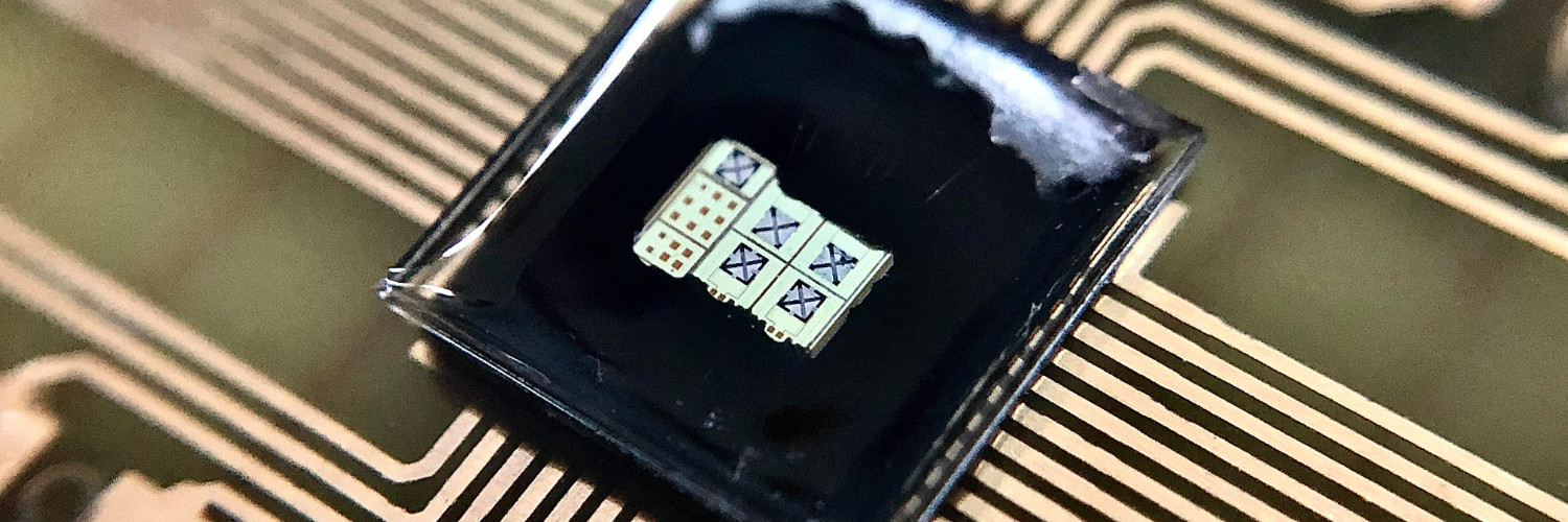
Thesis article : The CMOS-MEMS Electrostatic Transfer Head Integrated with Piezoresistive Force Sensor.
The chip is fabricated by TSMC process platform (0.18um 1P6M CMOS-MEMS). Due to this platform has the multi-layer structure, it makes the integration of sensor easier. This chip used poly-si as piezoresistive material, also set Wheatstone bridge to measure the change in resistance. The top metal layer is designed as electrode, it can generate electrostatic force to pick up the Micro LED chip while we applied voltage on it. Designed the via and sacrificed layer to fabricate the cavity, let poly-si has the space to deform. When the Micro LED chip contacted the transfer head, the poly-si would deform and we could do the measurement of resistance to calculate the bonding force. With this design, we can enhance the yield rate of mass transfer.
Bachelor’s Degree
・
Mechanical Engineering