
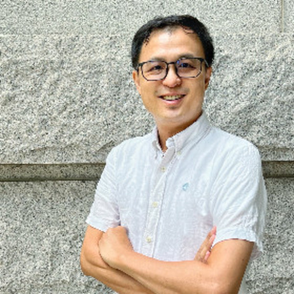
朱思明
Sr. Engineer
Motivated engineer who is highly energetic, outgoing and tenacity. Have project management experience. Ability to solve problems and rich cost down/capacity max out experience. Co-working with foreigners experience. Quickly learns and masters new concepts and skills.
Micron Technology 台灣美光
中原大學 Chung Yuan Christian University
Taichung, 台灣
Professional Background
- 現在の状況無職
- ProfessionSemiconductor Engineering・Research / R&D
- Fields半導体
- 職務経験10〜15年 (10〜15年関連の実務経験)
- Managementなし
- Skills
- LanguagesChinese・ネイティブまたはバイリンガルEnglish・中級者Japanese・初心者
- Highest level of educationMaster
Job search preferences
- Desired job typeフルタイム・リモートワークに興味あり
- Desired positionsSemiconductor Sr. Engineer, Manager
- 希望の勤務地Taiwan
- Freelance非フリーランス
Work Experience

OCT CPEE CVD/PVD Sr. Engineer
Taichung City, Taiwan
Integrate supplier resources to reduce company cost and improve capacity.

ADTT PVD Sr. Engineer
Taichung City, Taiwan
1.Published Micron internal paper in FY22.
2.TF line yield owner, and scrap wafer improve around 40%.
3.Contact Co/SICONI recipe optimization.
4.Digit line W sputter recipe development for RS reduction.
5.W/SIN capacity improve 5%~8% for max out project.

JTC Film Team Sr. Engineer
Taichung City, Taiwan
1.Development Ti/WN/WSI metal sputter recipe for digit line RS reduction
2.New tech process transfer form US RD team.

PEE PVD Sr. Engineer
Taichung City, Taiwan
1.SPC champion, responsible for PVD team meet SPC KPI.
2.Responsible backend layers defect/cost/max out projects.
3.TSV Cu process transfer from JP RD team.

TF Technology Development Engineer
Hsinchu City, Taiwan 300
1.Published paper “Capacitance density and breakdown voltage improvement by optimizing the PECVD dielectric film characteristics in metal insulator metal capacitors” in IEEE symposium 2015
2.Responsible for Logic Foundry Thin Film process development

TF Process Engineer
Hsinchu City, Taiwan 300
1.. NOR/NAND-Flash memory yield and capacity improvement.
2. Thin Film PVD/CVD Process maintenance.
3. CIP competition received Honorable Mention.
Education

Master’s Degree
・
物理活動・団体
童軍團, 攝影社,
詳細
“Percolation in Two-dimensional Nanoparticle Films from Colloidal Self-assembly” , 2007 , Physica Status Solidi (a) , vol.204 , p.1856-1862. (SCI期刊)
